Cadence Digital Design Flow Tutorial
First a schematic view of the circuit is created using the Cadence Composer Schematic Editor. We will be using a portion of the analog design flow which can handle up.

Analog Mixed Signal Group Wiki Digital Synthesis And Layout
It contains a complete skeleton the SKELETON directory using umc065 process as an example for you to do your own digital design from RTL HDL design all the way to physical layout for tape-out.
Cadence digital design flow tutorial. This tutorial will introduce the use of Cadence for simulating circuits in 6012. Digital Full Flow Cadences next-generation digital full flow platform adds new Genus and Innovus iSpatial unified physical optimization technology plus Machine Learning for improved PPA predictability and TAT. Creating a Schematic Cellview.
You learn several techniques to floorplan your design create partitions run place and route and optimize the design to close timing. In Tutorial 2 Using VLSI Flow Outputs you place-and-routed a 4-to-16 decoder imported the design into Cadence Virtuoso and investigated the di erence in timing and power. Here the command to launch the DFT flow is located at dftcordic_dft.
Hi guys. Design flows are broken into three types. Starting Cadence Virtuoso.
Our digital advanced-node flow helps you achieve the best Quality of Results QoR for challenging FinFET designs. Optimize designs using the physical synthesis flow. VLSIs Hello World you used the digital design ow to place-and-route a pre-existing library of standard cells based on an RTL description.
I would like to know the exact digital design flow for cadence. Starting from HDL down to GDSII. As a PCB designer it is valuable to have an understanding of the behind-the-scenes basics of electronic manufacturing workflow After all it is still heavily connected to electronics design.
Foundation Flow scripts. Creating a Symbol. Knowing what goes on in the manufacturing flow helps me to optimize my designs for better manufacturability.
Running the design-for-test DFT flow is very similar to the previous RTL compiler flow. Cadence is a suite of tools for IC design. First a schematic view of the circuit is created using the Cadence Composer Schematic Editor.
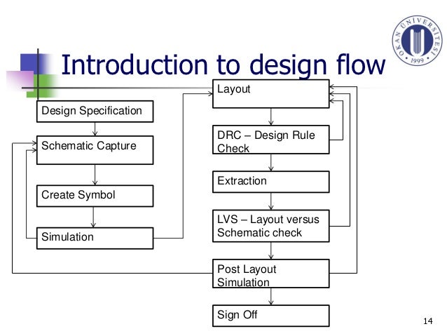
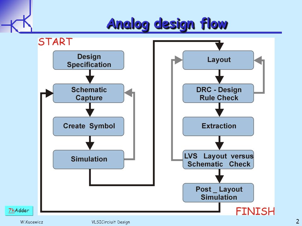
Fundamentals of IEEE1801 Low Power Specification. 1 shows the basic design flow of an analog IC design together with the Cadence tools required in each step. Innovus Implementation System Hierarchical In this course you explore the features of the Innovus Implementation System for creating and implementing a hierarchical design.
ANALOG IC DESIGN FLOW AND REQUIRED TOOLS Fig. This is a complete tutorial for you to get familiar with the standard digital design flow. Digital Analog Mixed Signal Choose a flow based on what the majority of your design will use.
This course is a complete tutorial for understanding the fundamentals of IEEE 1801 low power specification format concepts. It is the only platform built on a bedrock of superior signoff convergence with tightly integrated STA and IR-drop signoff. 3 Cadence Design Flows A design flow is from initial design conception to tape-out.
And a whole lot more. It allows for schematic capture simulation layout and post-layout verification of analog and digital designs. ASIC tools are much more separated.
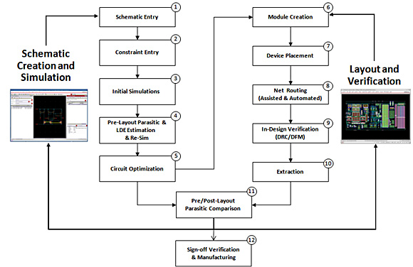
To participate you need to register. Design Rule Checking Layout Parameter Extraction Layout vs. Methodology for successful front-end design to back-end implementation of the chip at System on Chip SoC level.
It is also shown how the design. Cadence offers a variety of digital design flows that address these challenges. This involves using different tools from Synopsys and Cadence.
It actually uses the same tool and the scripts are setup in the same manner. 1 Cadence Virtuoso Logic Gates Tutorial. Standard Digital Design Flow.
Niques in an ASIC design flow with Synopsys Power CompilerAfterashort review of the sources of power consumption in a digital circuit tool-independent optimization techniques are presented for di erent abstraction levels. Our 3D-IC flow helps you address the synthesis floorplanning placement and routing challenges of digital and custom domains in a 3D-IC stack. ANALOG IC DESIGN FLOW AND REQUIRED TOOLS Fig.
In Tutorial 1 GCD. Schematic Comparison Introduction This document is one of a three-part tutorial for using CADENCE Custom IC Design Tools ver. This involves using different tools from Synopsys and Cadence.
Creating a Design Library. Forum focused on EDA software circuits schematics books theory papers asic pld 8051 DSP Network RF Analog Design PCB Service Manuals. Running the Design-for-Test Flow.
Apply the recommended synthesis flow using the Cadence Genus Synthesis Solution. Cadence Virtuoso Logic Gates Tutorial rev. 1 shows the basic design flow of an analog IC design together with the Cadence tools required in each step.
A step-by-step description of designing and testing an AND logic gate using Cadence Virtuoso. Alternatively a text netlist input can be employed. IC445 for a typical bottom-up digital circuit design flow with the AMI06 process technology and NCSU design kit.
In FPGA terms the design flow is broken into three stages with Xilinx and all integrated together.
Vlsi Cadence Tutorial Ahmet Ilker Sin
Introduction To Cadence Virtuoso Advanced Node Design Environment Custom Ic Design Cadence Blogs Cadence Community
Ece 5020 Class Homepage

Cadence Schematic Capture Tool Circuit Boards