De0 Nano Soc Tutorial
Students will create a hardware prototype in VHDL for the. Pilih Quartus Prime ModelSim dan device Cyclone V.
Atlas Soc Kits Terasic Technologies Mouser
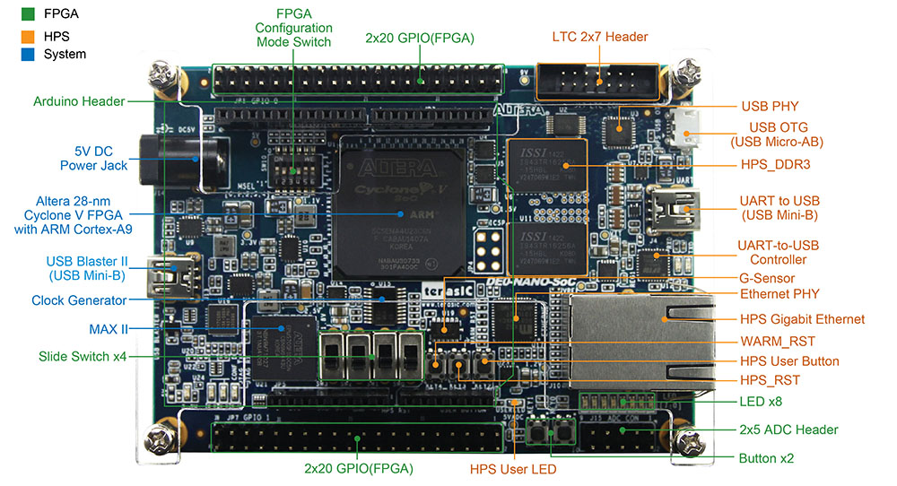
The Cyclone V SoC is a FPGA combined with a dual-core ARM Cortex-A9 hard processor system HPS and some peripherals.

De0 nano soc tutorial. Start Today and Become an Expert in Days. Kindly refer to Cyclone V DE0-Nano-SOC user guide Page 26. Get familiar with the source code used to execute the Fast Fourier Transform FFT in the Explore FFT Example.
The following sections provide a quick overview of the design flow explain what you need to get started and describe what you will learn. Pastikan file yang anda pilih sesuai dengan OS yang kamu gunakan. Check out the GPIO Example Application section to learn more about the 8 green user LEDs registered under the general-purpose inputoutput GPIO framework.
In this tutorial we are going to setup our first project of DE0-nano FPGA board. Download Quartus Prime di website Intel. Join Millions of Learners From Around The World Already Learning On Udemy.
Ad Learn SoC Online At Your Own Pace. Start Today and Become an Expert in Days. Pin 1 with GPIO 1 Pin 1.
The board is a good starting point to get involved in embedded system development with SoCs. Pada tutorial ini saya menggunakan OS Windows. Input pin and add a project description such as DE0-Nano Tutorial Project In this section you will make pin assignments.
Motherboard Terasic DE0-NANO-SoC User Manual 50 pages Motherboard Terasic DE0-Nano-SoC Getting Started Manual 26 pages Motherboard Terasic DE0-CV User Manual. For demonstration purposes we are going to implement a Full Adder logic circuit. Join Millions of Learners From Around The World Already Learning On Udemy.
Ad Learn SoC Online At Your Own Pace. The DE0-Nano-SoC Development Kit contains all the tools needed to use the board in conjunction with a computer that runs the Microsoft Windows XP or later. CV DE0-NANO-SOC GPIO Pin Arrangement originally from here.
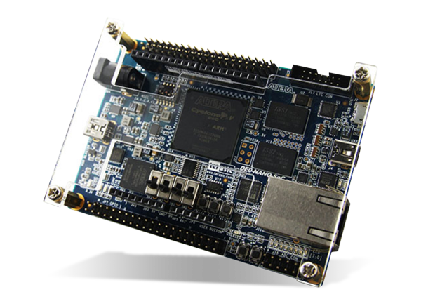
This is one of the most powerful and affordable FPGA boards available in the Market. Figure 3-18 from this document can be seen in Figure 2. The following hardware is provided on the board.
The DE0-Nano-SoC development board is equipped with high-speed DDR3 memory analog to digital capabilities Ethernet networking and much more that promise many exciting applications. I2C FPGA Tutorial Terasic Technologies Strategic Marketing Manager Allen Houng In this tutorial video we perform a write operation on the EEPROM chip on the DE0-Nano. Download file De0-Nano-SoC Manual untuk mengetahui lebih lanjut tentang spesifikasi dari DE0 Nano SoC.
Adding tasks to Linux Initialization using inittab - DE0-NANO-SOC Boards NIOS-IIe Gen2 processors and FreeRTOSv900 in Quartus 1700 DE0-NANO Nios II Hardware Arduino - DE0-NANO-SOC DE0-NANO-SOC LCD DriverPSP Screen Using Nios II Turning On qsys debug messages Generador de efectos de audio utilizando HDL Coder de simulink. Before making pin assignments perform the. This section contains tutorial projects for the Terasic DE10-Nano board.
Tutorial for using the DE1-SoCDE0-Nano-SoC boards for bare-metal and linux programming License. Terasic DE10-Nano Tutorial Projects. Recently I bought the DE0-Nano-SoC KitAtlas-SoC development board from Terasic which contains a Cyclone V SoC from Altera.
This tutorial provides comprehensive information that will help you understand how to create a FPGA design and run it on your DE0-Nano-SoC development board. In this tutorial we will take a look on how a regular RGB LED matrix function and how to interface it with your FPGA boardEnjoyMusic. The purpose of this lab is to introduce students to the HPSFPGA design flow involved in SoCdesign using the DE1-SoC development board.
Getting Started With De0 Nano Soc Fpga

Terasic De Boards De0 Nano Soc Kit Atlas Soc Kit
Getting Started With De0 Nano Soc Fpga

Getting Started With De0 Nano Soc Fpga
